
This is continuing of the thread of making AVR controlled signal generator. This section is devoted to 1 layer PCB prototype making using ultraviolet light exposure and etching.
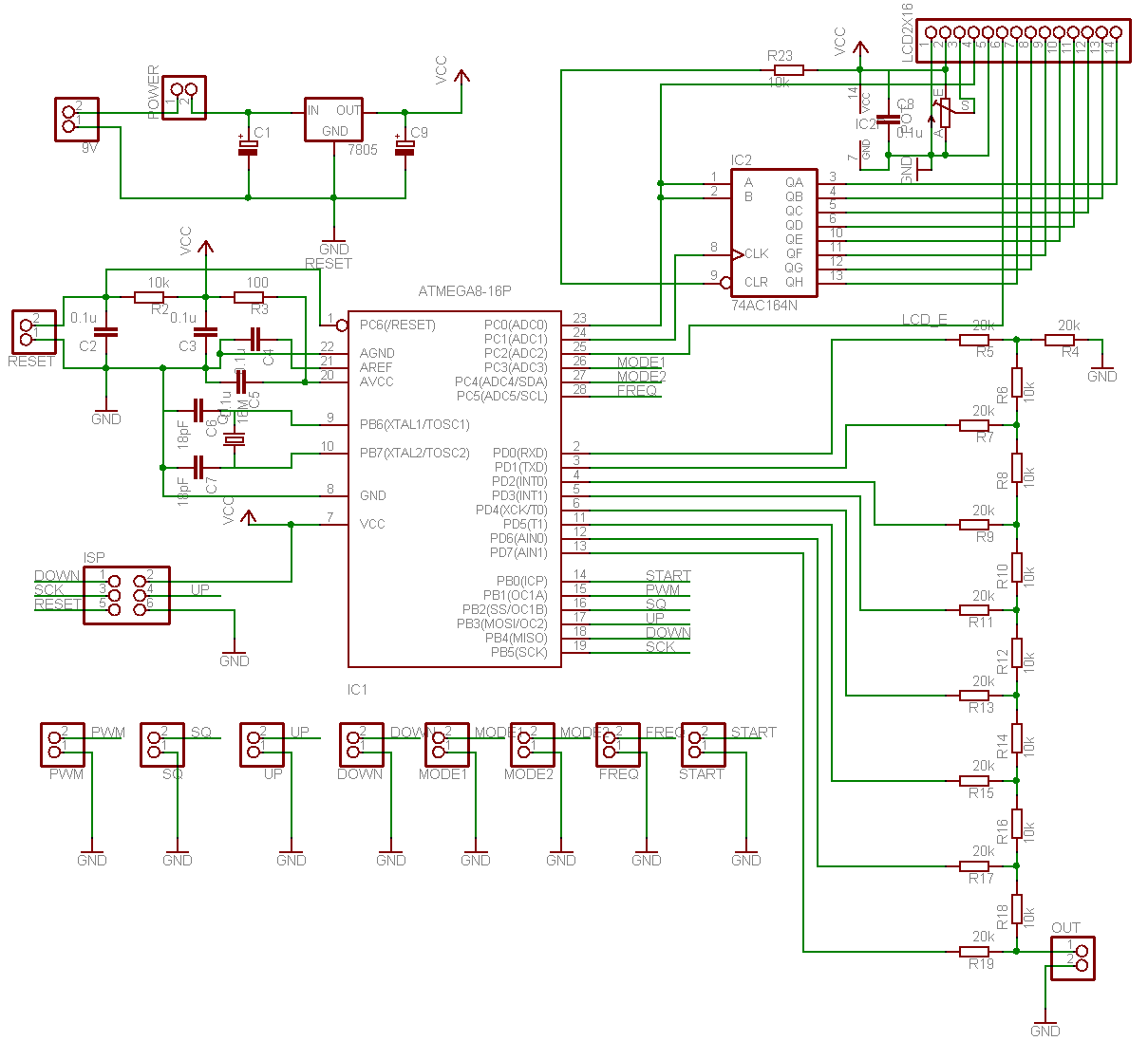
I’ve chosen Eagle as PCB designing software. This is convenient software for making hobby circuits. First, I designed a circuit of AVR controlled signal generator:
When Circuit is designed, then follows PCB tracing. The resulting PCB I got is here:

Not all traces were routed. I will need to connect some places with wires because there left some traces unrouted.
For PCB making, I am using the board already covered with the photosensitive layer. You may buy them in the market:

You have to peel the protective layer and expose through the mask:

Masked PCB:

After UV exposure, the second phase is development. I used Sodium Metasilicate as a developer: Sodium Metasilicate
This is a better choice than NaOH. It is less aggressive, and it is not critical to temperature or concentration. Add 50g for one liter of water. The temperature of the solution should be in the range of 18 – 24 degrees of Celsius. Develop about 1 – 2 minutes.

After PCB is developed, then wash with water and dry. Then put in an etching solution (Ammonium Persulphate). Add about 200 – 250g for one liter of water. The temperature of the etching liquid should be about 40 – 50 degrees of Celsius (instead, you can use FeCl3, but it is a very messy chemical) :

After the board is finished, clean the board with abrasive or developer. I use acetone as it cleans faster, but also it stinks badly. Better do it outside the house.

After the board is done, inspect if there are any interconnections between tracks. In my case, there are some because the mask wasn’t printed very well, and probably there was a gap between mask and board left during exposure. The best way to do corrections is to use a sharp knife or needle.
Then drill the holes, and it is ok to solder.
Hi,
I noticed your method for making the boards is fairly complicated. I’m using an etching process that requires less expensive materials, and no optical exposure. You might want to give it a try (laser printer + glossy photo paper to make the resist mask).
Francis
I am using both methods laser printer and UV exposure. It depends on PCB I’ve been making PCB where track were 0.2mm wide. I don’t think laser printer method could do this. Of course this particular PCB can be made with laser printer and glossy paper. Sometimes my decision depends on materials I have near by 🙂