
How repeatedly make good PCB? Many hobbyists face this issue every time they are prototyping their ideas. Designing the PCB layout (it doesn’t matter it is a through-hole or surface mount) may be a tricky task, especially when dealing with dimensions like 0.2mm tracks or 0.5mm surface-mount pitches. A laser printer, plotting, or other similar transfer technologies can’t deal with such dimensions.
After I have tried the photographic method of PCB artwork transfer, I don’t even want to touch the Iron and laser printer. Using photosensitive laminate and single transparent media, I can repeatedly make any number of PCBs. The benefits of using photographic methods are as follows:
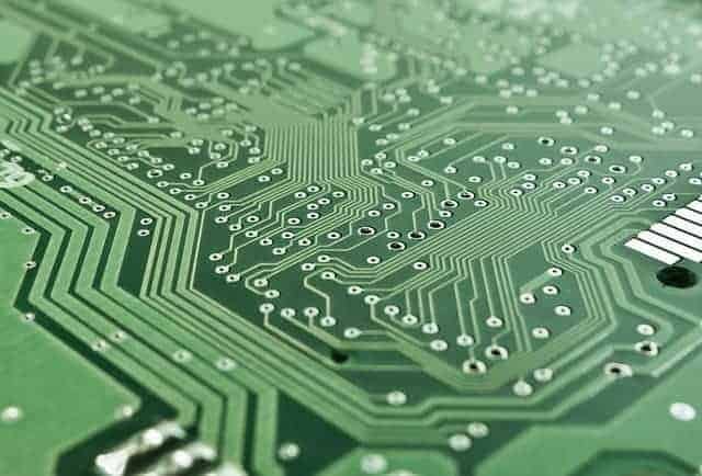
Pay the biggest attention to artwork fabrication. Without good artwork, you won’t be able to make a good PCB. From My experience, I can say that I always make small mistakes with PCB artworks, and I spot them usually after PCB is etched. Devote more time for PCB artwork tracing, and you will save much more time while soldering.
- Transferred artwork is obvious; edges are smooth;
- Track thickness may be up to 0.2mm or even less with good mask quality, made with a good laser printer (usually a new one). After printer cartridge refill – printing quality drops down;
- With one artwork mask, I can clone many PCBs;
The artwork should be:
- Clear;
- Sharp;
- Solid black when printed.
- The printed side should be in contact with PCB, so don’t put the opposite as then you get a blurred picture.
For Artwork transfer, it is not necessary to use transparent media. Paper (UV translucent) can be good too. It may require longer exposure. Why am I saying this? Because laser printers like paper more than acetate film. The toner stays flattered on paper, and black is smoother than on film. Especially using printers with refilled cartridges, I would recommend use paper instead of film. I used to use film, but the results are rather disappointing than promising.
The printer itself should have following:
- Resolution at least 600 dpi;
- Should print good solid black with no toner holes;
- Pint accuracy should be good, especially when printing double-sided PCB artwork;
The next important thing in PCB development is Photoresist PCB laminate. It has to be of good quality, especially when dealing with small tracks. If you use a pre-coated PCB, inspect if there are no scratches in the covering and check the PCB age. When handling, just avoid direct sunlight and unnecessary light exposure. And develop just after exposure. If you decide to spray photoresist by yourself, remember that area should be clean from dust. It works for low-resolution boards, but for higher resolution, I would recommend buying pre-coated boards.
Exposing of photoresistive boards are done under Ultraviolet lamps. This is not a very critical issue, but still:
- Don’t use shortwave lamps;
- Use more tubes than one – this makes the light more even;
- Use a timer to make exact exposure timing.
For developing boards, I don’t recommend using sodium hydroxide. This is dreadful stuff. It is sensitive to temperature and concentration, and it is an aggressive chemical. It may easily strip all photoresist. The solution doesn’t last long. Better use silicate-based products. This isn’t sensitive to temperature or concentration. It is hard to overdevelop. Solution lasts much longer, and you can make stronger solutions for faster development. This would be your PCB killing by using sodium hydroxide.
Fro etching, I would not recommend using ferric chloride. This is really messy stuff. But if so, then avoid any contact with metal as it attacks almost any metal. Use plastic or glass tank as a better alternative use Ammonium persulphate. As this is a transparent solution, it doesn’t mess, and it is not aggressive as ferric chloride. But it gives an even better result in etching. It usually doesn’t etch under the track what is important when the board is high resolution.
These are only general guidelines for making PCB. Further, I would recommend reading the following sources:
AVR controlled signal generator-1 layer PCB prototype
The IBM range is designed specifically for HP laser printers and covers 70% of the entire HP range. The IBM cartridges cost less than original HP cartridges, provide IBM print quality, and are significantly better for the environment.