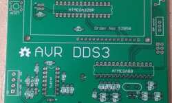
Category Archives: AVR controlled signal generator

AVR controlled signal generator

Modeling of analog part for DDS3 signal generator

When building AVR DDS2 signal generator there were lots of discussions about signal conditioning in analog part of device. First argument was that LM358 wasn’t the best choice for this purpose. Another one pointed to sine wave that weren’t smooth enough.

As you can see there are some dents on it. Other waveforms also are distorted especially when higher voltages are selected. This definitely asks for better analog part. Some people suggested to replace LM358 with OPA2134, but it seems to be quite expensive choice. In my opinion low noise general purpose op-amp can be great too. I’m gonna give a try to Texas Instruments TL074 low noise op-amp. It is low power, high slew rate (13V/us) IC – almost five times faster than LM358 and for same reasonable price. Continue reading

AVR DDS signal generator V2.0

Finally second and improved AVR DDS signal generator is here. First AVR DDS V1.0 generator was only an attempt of running DDS algorithm without any amplitude control. This time I still wanted to keep things simple like minimum count of widely accessible components circuit, single sided PCB that comes together with good functionality.

AVR_DDS_signal_generator_V2_0.jpg

AVR DDS specification

AVR DDS signal generator V2.0 is a firmware based DDS signal generator which uses slightly modified Jesper’s DDS algorithm adapted to AVR-GCC C program as in-line ASM. Signal generator has two outputs – one for DDS signal and another for high speed [1..8MHz] square signal – which may be used for reliving microcontrollers with wrong fuse settings or for other purposes as well. High speed (HS) signal is direct output from Atmega16 OC1A(PD5) pin. DDS output is used for all other signals that are generated via R2R resistor network and is adjusted via LM358N offset and amplitude regulating circuits. Offset and amplitude can be regulated by two potentiometers. Offset can be regulated in range +5V..-5V while amplitude in range 0..10V. DDS frequency range is from 0 to 65534Hz that is more than enough for testing audio circuits and other tasks.

Main AVR DDS V2.0 signal generator features:

  • Simple circuit with easily accessible and cheap components;
  • Single sided PCB;
  • In box power supply with external AC plug;
  • Dedicated high speed (HS) signal output up to 8MHz;
  • DDS signal with variable amplitude and offset;
  • DDS signals: sine, square, saw, rev saw, triangle, ECG and noise.
  • 2×16 LCD menu;
  • Intuitive 5 button keypad.
  • Frequency adjusting steps: 1, 10, 100, 1000, 10000Hz;
  • Restoring last configuration after power up.

Continue reading

AVR-DDS signal generator in-line ASM explained

I have got a couple of questions (in fact not a first ones) for AVR DDS generator I have built:

“that’s all the asm code that I don’t understand.

Could you explain it? Is it possible to do it without inline asm (only in C)?”

I decided to explain this part more deeply. Because it took some time for myself to figure this all out.

First of all what wee have to do… it is to implement simple DDS algorithm. Read about it for example here: http://www.hit.bme.hu/~papay/sci/DDS/start.htm

In few words Direct Digital Synthesis(DDS) is known as Numerically Controlled Oscillator. Simple rule: NCO-based DDS is a point(memory location)-skipping technique (and a constant interpolation of the stored signal) and runs at constant update(clock)-rate. As the DDS output frequency is increased, the number of samples per waveform cycles decreases.

dds1.GIF

Practically speaking lets have some math. We have clock generator connected to MCU. In my case F_CPU=16000000Hz. This is our Clock In.

Then we have sinewave map stored in rom:

const uint8_t sinewave[] __attribute__ ((section (“.MySection1″)))= //256 values

{0×80,0×83,0×86,0×89,0x8c,0x8f,0×92,…

If we have 256 values of sine wave for single period, then at clock rate 16MHz picking each value from table we would have max sine wave frequency Fsine=16000000/256=64kHz; This would be ok. But what if wee need to have sinewave frequency 1kHz or 1MHz. Then wee need to implement some memory location skipping technique – this is what DDS does.

If we would like to have 128kHz instead of 64kKz we would pick every second sample from sinewave rom map (128 samples). And if we would like to have 32kHz we would have to make a delay after each sample and so on. DDS makes this much easier by having Phase accumulator.

dds2.gif
In my case phase accumulator is 24bit variable. Phase accumulator is calculating address to sinewave table. Now all matters only in delta phase adder calculation:Firs of all calculate output frequency resolution:fres=(F_CPU/(clocks for one sample output))/2^(accumulator length) = 16000000/9/2^24=0.1059638129340278Hz.

Now ir is simple to calculate phase accumulator adder value. If wee need signal frequency

Fsignal=Acc_adder*fres; For instance if you need 1kHz output, then;

Acc_adder=1000/0.1059638129340278=9437.18399(9)=9437.

In my code I have used value frequency to calculate phase accumulator adder:

temp=frequency/RESOLUTION;

tfreq1=(uint8_t)(temp);

tfreq2=(uint8_t)(temp>>8);

tfreq3=(uint8_t)(temp>>16);

In pure assembly language this should look like:

ldi    r31,hi8(sinewave)   ; setup Z pointer hi
ldi    r30,lo8(sinewave)   ; setup Z pointer lo

; clear accumulator

ldi     r29,0x00        ; clear accumulator
ldi     r28,0x00        ; clear accumulator

; setup adder value  to 1 kHz
ldi     r24,tfreq1      ; tfreq1->r24
ldi     r25,tfreq2      ; tfreq2->r25
ldi     r26,tfreq2      ; tfreq2->r26
LOOP1:
add     r28,r24         ; 1
adc     r29,r25         ; 1
adc     r30,r26         ; 1 (Z pointer updated)
lpm                     ; 3 (load for sinewave table)
out     PORTD,r0        ; 1 (out to D port)
rjmp    LOOP1           ; 2 => 9 cycles

I think ASM code explains why it is hard to do in only C language – it is hard control number of cycles in main loop. Compiler output code may differ from expected and may not be optimal. Its all about performance. You can implement DDS algorithm in C language, but this probably would give lower frequency resolution than in-line ASM.

Lets start from explaining Inline ASM I have used. Inline ASM is a same ASM languge, but ithas to be written with some rules that compiler could understand. There are many things you have to have in mind. Like using static inline function declaration and so on.

For in-line ASM read http://www.nongnu.org/avr-libc/user-manual/inline_asm.html

void static inline signalOUT(const uint8_t *signal, uint8_t ad2, uint8_t ad1, uint8_t ad0)

{

asm volatile( “eor r18, r18 ;r18<-0" "\n\t"

“eor r19, r19 ;r19<-0" "\n\t"

“1:” “\n\t”

“add r18, %0 ;1 cycle” “\n\t”

“adc r19, %1 ;1 cycle” “\n\t”

“adc %A3, %2 ;1 cycle” “\n\t”

“lpm ;3 cycles” “\n\t”

“out %4, __tmp_reg__ ;1 cycle” “\n\t”

“rjmp 1b ;2 cycles. Total 9 cycles” “\n\t”

:

:”r” (ad0),”r” (ad1),”r” (ad2),”e” (signal),”I” (_SFR_IO_ADDR(PORTD))

:”r18″, “r19″

);

}

In this particular case I will use explain each line of code:

  • void static inline signalOUT(const uint8_t *signal, uint8_t ad2, uint8_t ad1, uint8_t ad0) – This is function declaration which is called like signalOUT(sinewave,tfreq3, tfreq2, tfreq1); sinewave is lookup table pointer, tfreq3, tfreq2, tfreq1 – are 24 bit accumulato adder value split in 8 byte variables.

  • asm volatile(“ ”); - this is how asm inline is included in code(volatile switches off compiler optimization);

  • “eor r18, r18 ;r18<-0" "\n\t” – writes 0 to r18 (“\n\t” – used for cleaner listing new line and tab);

  • “eor r19, r19 ;r19<-0" "\n\t" - writes 0 to r19;

  • “1:” - label;

  • “add r18, %0 “ – means add (ad0) variable tfreq1 to r18 (tfreq1 is tied to register :”r” (ad0));

  • “adc r19, %1” – means adc (ad1) variable tfreq2 to r19 (tfreq2 is tied to register :”r” (ad1));

  • “adc %A3, %2” – means adc (ad2) variable tfreq3 to r30 (tfreq3 is tied to register :”r” (ad2)) and %A3 means r30 that :”e” (signal) declares register pair Z tied to pointer signal;

  • lpm – is obvious load byte to r0 from Z pointed location of Flash.

  • “out %4, __tmp_reg__” – means that %4 variable is declared by :”I” (_SFR_IO_ADDR(PORTD)); __tmp_reg__ is by default as r0;

  • “rjmp 1b” – jump to 1: in unix style;

  • : – defines output operands

  • :”r” (ad0),”r” (ad1),”r” (ad2),”e” (signal),”I” (_SFR_IO_ADDR(PORTD)) – input operands

  • :”r18″, “r19″ – clobber lists (define register that are not passed as operands).

Last notice that declaring simple function without static inline generates ASM code where pointer signal is passed not to R30:R31 register pair but to R24:R25.

I don’t know if this made things more clear. If not search www before asking. One of starting points would be http://www.myplace.nu/avr/minidds/index.htm.

Good luck.

AVR DDS signal generator V1.0

Sometimes when tuning various electronic hardware we need simple signal generator with various waveform and frequency. One of the options is to by a professional with variable gain professional coating and many additional functions. But if you are an amateur you might want to build one. This small project is dedicated for building one of those signal generators.

LCD_Panel


Specification

AVR DDS signal generator consists of following parts:

  • Atmel Atmega8 8 bit microcontroller;
  • Supply source and voltage regulator;
  • 2×16 standard LCD and shift register 74HC164;
  • 7 buttons;
  • R-2R resistor leader for DAC;
  • Three outputs: universal(OUT) from DAC, PWM and pulses;
  • Metal case;
  • and microcontroller firmware.

Atmega8 microcontroller is a simplest of atmega series. There is 8kb of FLASH program memory, maximum frequency is 16MHz, which is used to reach DDS generators maximum resolution at maximum frequency. For know frequency is limited from 1 to 65535Hz with minimal step of 1Hz.

DDS AVR generator is powered with 9V battery. Voltage is reduces to 5V and stabilized by 7805 voltage regulator.

LCD is controlled using three wires through shift register 74HC164. So this register is used as serial to parallel converter in order to save microcontroller pins. LCD is controlled in 8 bit mode.

AVR DDS Generator uses 7 control buttons:

  • Start;

  • Stop, which is a reset also;

  • IP- increasing value;

  • DOWN- decreasing value;

  • Mode1 – signal selection button;

  • Mode2 – signal properties;

  • Freq – signal frequency multiplier selection.

  • Buttons on the box

AVR DDS signal generator uses R-2R digital to analog (DAC) converter This is a simplest solution where resistors are connected in a ladder:

R-2R_ledder


In this schematic R=10kohm. By using 8 bits and 5V step value is about 18.5mV. This is enough for getting average quality signals.

Generator has three outputs:

  • Universal DAC output through R-2R ladder;
  • PWM;
  • Impulse (SQ);

Universal output (OUT) is a signal output from DAC. This output is to form various signals like sawtooth, sine, square, triangle.

PWM channel is used to form for PWM signal output – directly from timer.

SQ channel is additional channel to form square pulses or second PWM signal. Will be implemented in future.

AVR_DDS_diagram


In the block chart is described the structure of AVD DDS signal generator. You can se the signal paths. Each block part is described in specification.

Menu and program stages:

After generator is switched on the message is displayed in LCD: LCD SCREENS


„Mode2“ button selects the step of frequency from 1 to 10000Hz by pressing it in series. “Up” and “Down” buttons change the frequency value by step value.

After “Start” button is pressed – last settings are saved in EEPROM and signal generation is started.

Above functionality is implemented and tested. In a future plans there are few more signal generation modes. By pressing “Mode1” you can see following screens whish may change a little during implementation:LCD Screens1


Circuit diagram and PCB

PCB is single sided with some wiring done in top side.

pcb.jpg

schematics.png


Circuit diagram explanation:

Microcontroller port pins are connected to:

  • R-2R DAC is connected to D port pins 0…7;
  • Shift register data line is connected to C port’s 0 pin;
  • Shift registers synchronize line is connected to port C pin ;
  • LCD screen’s E signal is controlled by C ports pin 2;
  • Start button is connected to B port pin 0;
  • Stop button is reset button;
  • Up button is connected to port B pin 3;
  • Down button is connected to port B pin 4;
  • Mode1 button is connected to C port pin 3;
  • Mode2 button is connected to C port pin 4;
  • Freq button is connected to C port pin 5;
  • SQ signal is coming from AVR b port pin 2;
  • PWM signal comes out from Port B pin 1.

Part list (exported from eagle):Parts List

Tools used

In developing this AVR DDS signal generator There were following tools used:

Software:

Hardware tools:

Few words about firmware

Program is written in C language and can be compiled with WinAVR20060421 toolset. Programming is done by using AVR ISP and PonyProg programming software.

Program flow in few words:

When AVR DDS generator is switched on:

  • Initialization of LCD;
  • Reading previous settings from EEPROM memory and displaying to LCD;
  • Using buttons settings and signals can be changed. When “Start” button is pressed, new settings are saved to EEPROM and signal generation starts.
  • Note: After power up you can press “Start” to start last saved signal generation immediately;
  • Generator is stopped by pressing Stop button which resets the generator. After Reset generator again loads its lasts configuration from EEPROM memory and is ready to start new generation.

EEPROM memory stores following data:EEPROM data

Mode values:

  • 0 – OUT_|¯|_;
  • 1 – OUT|/|/|;
  • 2 – OUT|\|\|;
  • 3 – OUT/\/\/\;
  • 4 – OUT~~~~;
  • 5 – OUT-NOISE;
  • 20 – PWM-OCC;
  • 21 – PWM-SINMDS;
  • 22 – PWMSQSMDS;
  • 23 – PWM-CMDS;

Frequency value is divided to 3 EEPROM bytes. Because max theoretical frequency is 16MHz whis hexadecimal value is 0XF42400:

Freq[23...16]

Freq[16...8]

Freq[7...0]

Duty value is from 1 to 99 in percents.

Program Structure:

LCD_3w.h – LCD settings

LCD_3w.c it contains LCD control functions

  • void sendByteToRegister(uint8_t);
  • void LCDenableCommand(void);
  • void LCDdisableCommand(void);
  • void LCDenableData(void);
  • void LCDdisableData(void);
  • void LCDsendChar(uint8_t); //forms data ready to send to 74HC164
  • void LCDsendCommand(uint8_t); //forms data ready to send to 74HC164
  • void LCDinit(void);
  • void LCDwritebyte(uint8_t, uint8_t);
  • void LCDdefinechar(const uint8_t* ,uint8_t);
  • void LCDclr(void);
  • void LCDhome(void);
  • void LCDstring(uint8_t*, uint8_t);
  • void LCDGotoXY(uint8_t, uint8_t);

main.c – main program text where:

  • signal tables are stored;
  • messages to LCD are described
  • EEPROM initialization is done;
  • changing parameters are implemented;
  • signal generation (using in-line ASM routines) is performed.

Testing

For now testing is done by using frequency counter and Oscilloscope. In a frequency range of 1 to 65535Hz works OK. There can be greater frequency range programmed but with less resolution. I think for audio equipment testing there is more than enough frequencies.

AVR_DDS_Signals

Discussion

As I mentioned earlier, this is a first trimmed version of AVR controlled generator. It has half of working functionality in many cases this can be enough. Main signals are generated and can be controlled. In a future the functionality can be expanded to add PWM generation using timers. Generator generates signals as they are – directly from DAC. There is no variable gain regulation. To be more interesting project there can be VGA amplifier used with feedback to control output signal voltage. The project source code is open to modify and expand functionality. If there will be some good modifications – feedback is always welcome.

You can download AVR DDS Documentation and AVR DDS Source files as they are.

More pictures from the project:

AVRDDS1 AVRDDS2

AVRDDS3 AVRDDS4

AVRDDS5 AVRDDS6

AVRDDS7 AVRDDS8

Download Eagle project files

Some software writing ideas were taken from Jespers Mini DDS.


AVR controlled DDS generator software writing

During my spare time I am developing the program for AVR controlled DDS generator. I decided to write software using WinAVR tool-set. How far ahead I have moved with this?

I have implemented:

  • Menu system;
  • Reading previous generator configuration from EEPROM;
  • Setting signal mode;
  • Storing last generator configuration to EEPROM to be loaded after reset;
  • Four types of signal output (square, sawtooth, triangle and sine wave);

Still need to do:

  • Ability to change signal frequency;
  • Implement other signals (listed bellow);
  • Make program clean-up;

Signals in AVR controlled generator:

  • 0 – OUT_|¯|_ – square wave(done);
  • 1 – OUT|/|/| – sawtooth(done);
  • 2 – OUT|\|\| – reverse sawtooth(awaiting);
  • 3 – OUT/\/\/\ – triangle(done);
  • 4 – OUT~~~~ – sine wave(done);
  • 5 – OUT-NOISE – noise signal(awaiting);
  • 20 – PWM-OCC – timer output compare mode(awaiting);
  • 21 – PWM-SINMDS – sine wave modulated PWM(awaiting);
  • 22 – PWMSQSMDS – sine wave modulated PWM. PWM positive, SQ – negative polarity(awaiting);
  • 23 – PWM-CMDS – custom PWM. Will be possible to set custom duty cycle(awaiting);

Signal generation

Square, sawtooth, triangle and sine waves are generated by reading values from flash memory. Fragment of sine wave is as follows:

//———————————————–

//signals saved in flash memory

const uint8_t sinewave[] PROGMEM= //256 values

{

0×80,0×83,0×86,0×89,0x8c,0x8f,0×92,0×95,0×98,0x9c,0x9f,0xa2,0xa5,0xa8,0xab,0xae,

0xb0,0xb3,0xb6,0xb9,0xbc,0xbf,0xc1,0xc4,0xc7,0xc9,0xcc,0xce,0xd1,0xd3,0xd5,0xd8,

0xda,0xdc,0xde,0xe0,0xe2,0xe4,0xe6,0xe8,0xea,0xec,0xed,0xef,0xf0,0xf2,0xf3,0xf5,

0xf6,0xf7,0xf8,0xf9,0xfa,0xfb,0xfc,0xfc,0xfd,0xfe,0xfe,0xff,0xff,0xff,0xff,0xff,

0xff,0xff,0xff,0xff,0xff,0xff,0xfe,0xfe,0xfd,0xfc,0xfc,0xfb,0xfa,0xf9,0xf8,0xf7,

0xf6,0xf5,0xf3,0xf2,0xf0,0xef,0xed,0xec,0xea,0xe8,0xe6,0xe4,0xe2,0xe0,0xde,0xdc,

0xda,0xd8,0xd5,0xd3,0xd1,0xce,0xcc,0xc9,0xc7,0xc4,0xc1,0xbf,0xbc,0xb9,0xb6,0xb3,

0xb0,0xae,0xab,0xa8,0xa5,0xa2,0x9f,0x9c,0×98,0×95,0×92,0x8f,0x8c,0×89,0×86,0×83,

0×80,0x7c,0×79,0×76,0×73,0×70,0x6d,0x6a,0×67,0×63,0×60,0x5d,0x5a,0×57,0×54,0×51,

0x4f,0x4c,0×49,0×46,0×43,0×40,0x3e,0x3b,0×38,0×36,0×33,0×31,0x2e,0x2c,0x2a,0×27,

0×25,0×23,0×21,0x1f,0x1d,0x1b,0×19,0×17,0×15,0×13,0×12,0×10,0x0f,0x0d,0x0c,0x0a,

0×09,0×08,0×07,0×06,0×05,0×04,0×03,0×03,0×02,0×01,0×01,0×00,0×00,0×00,0×00,0×00,

0×00,0×00,0×00,0×00,0×00,0×00,0×01,0×01,0×02,0×03,0×03,0×04,0×05,0×06,0×07,0×08,

0×09,0x0a,0x0c,0x0d,0x0f,0×10,0×12,0×13,0×15,0×17,0×19,0x1b,0x1d,0x1f,0×21,0×23,

0×25,0×27,0x2a,0x2c,0x2e,0×31,0×33,0×36,0×38,0x3b,0x3e,0×40,0×43,0×46,0×49,0x4c,

0x4f,0×51,0×54,0×57,0x5a,0x5d,0×60,0×63,0×67,0x6a,0x6d,0×70,0×73,0×76,0×79,0x7c

};

//———————————————–

The same is with square, sawtooth and triangle. Each wave is stored using 256 value table.

Signal is generated using simple function:

//———————————————–

void signalOUT(const uint8_t *signal)

{

uint8_t i;

i=0;

do

{

PORTD=pgm_read_byte(&signal[i++]);

}while(1);

}

//———————————————–

Using this function the maximum generated signal frequency was 6,25kHz. This means that one signal period consists of 256 values from signal table. Crystal frequency is 16MHz. So for one value from table it requires 16000000/(6250*256)=10 clock cycles.

Changing frequency of those signals should be ease. Just insert inside loop delay function regarding to selected frequency. This I will do later.

I still don’t know is it worse to try increase maximum frequency of signal. Now it is 6,25kHz and takes 10 clock cycles for one byte from 256 to output. If I would reach 5 cycles, that would be double frequency 12,5kHz.

In other hand if greater frequencies are needed there will be possibility to use timer signal generator on output compare mode, but only square waves.

Now I going to focus on implementing what I have planned and then think about optimisation.

Bellow are signal pictures I have got at frequency 6,25kHz(picture quality is poor – I really need to get tripod for my camera):

Square_signal.jpg

Square

sawtooth_signal.jpg

Sawtooth

triangle_signal.jpg

Triangle

sine_signal.jpg

Sine wave

The source code of current program is here:AVR controlled DDS generator software

Full documentation is on its way.

Creating custom LCD characters using WinAVR

Standard LCD modules comes with built in Character MAP stored in LCD ROM memory. There is plenty of characters for your needs, but still you may need some special ones like backslashes, or some symbols that are in different languages. For this LCD has a reserved RAM area for storing eight 5×7 dot matrix character patterns.

hd44780-charset.png

In the table above this area is in first column with addresses starting from 0 to 7 (from 0b00000000 to 0b00000111). This means, that you can define any type of characters in these 8 fields as you like and use them by calling them by addresses from 0 to 7.

To define one character, you will need to write eight bytes in row to CGRAM memory

For 0 character address (DDRAM=0):

custchar.JPG

So for the first character creation procedure would be:

Cycle of 8 iterations:

Send command to LCD with CGRAM address from 40h to 47h;

Send bytes to to selected CGRAM address

Because characters are 5×7 dots. You only need to modify first five bits of each byte. Other area fill with zeros(Marked blue in picture).

For other 7 characters the procedure is the same. Continue on next 8 CGRAM addresses 48h-4Fh. the last CGRAM address for eighth character is l 78h.

So you can create an array of 64bytes and write them all at once to CGRAM. Then you can read separate characters using DDRAM addresses from 0 to 7.

Before load your custom character to CGRAM, you need to store these chunks of 8 bytes.

The best way to store is program memory (FLASH).

const uint8_t squareR[] PROGMEM=

{

0b00011110,

0b00000010,

0b00000010,

0b00000010,

0b00000010,

0b00000011,

0b00000000,

0b00000000

};

Construction const uint8_t squareR[] PROGMEM menas that data is stored in FLASH at address squareR. For this to work you must include #include „avr/pgmspace.h“ library.

Then reading from program memory is ease pgm_read_byte(squareR[0] ):

Sending to custom character to LCD would look like:

void LCDdefinechar(const uint8_t *pc,uint8_t char_code){

uint8_t a, pcc;

uint16_t i;

a=(char_code<<3)|0x40;//calculate CGRAM address respectively to DDRAM address

for (i=0; i<8; i++){ //eight bytes for one character

pcc=pgm_read_byte(&pc[i]);//reads byte from program memory

LCDwritebyte(a++,pcc); //writes byte to CGRAM at address a

}

Function LCDwritebyte () is simple. Send command with CGRAM address to LCD and after send a byte.

void LCDwritebyte(uint8_t a, uint8_t pc)

{

LCDsendCommand(a);

LCDsendChar(pc);

}

Displaying first custom character stored in DDRAM address 0 is simple:

LCDsendChar(0);

Realization of functions

LCDsendCommand(a);

LCDsendChar(pc);

Depends on how you connect your LCD. I have developed simple routines for 3-wire LCD connection. You may download them from here:LCD Custom char with WinAVR . This is a part of project AVR controlled generator which is still in development stage.

AVR controlled signal generator-first impression

Lazy evening. I decided to take couple shots of couple generated signals. Without going to deep in to timings I wrote couple algorithms to make sure the signals are generated correctly at all voltage range 0-5V.

First is Sawtooth signal using asm in AVRStudio:

.INCLUDE “m8def.inc”

.DEF tmp = R16 ; Multipurpose register

ldi tmp,0xFF; Set all pins of Port D as output

out DDRD,tmp

sawtooth:

out PORTD,tmp

inc tmp

rjmp sawtooth

Sawtooth.jpg
(My oscilloscope is really old so sorry for bad quality)

Second signal Triangle. This one I programmed using WinAVR toolset.

int main (void)

{

uint8_t x=0, y=0;

atmega8init();

for (;;) /* Note [6] */

{

if (y==0)

{

x++;

if (x==255) y=1;

}

else

{

x–;

if (x==0) y=0;

}

PORTD=x;

}

return (0);

}

Triangle.jpg

It is obvious that signals are generated correctly at all voltage interval 0-5V.

Later I will probably use signal (pulse, sawtooth, triangle, and sinusoid) tables stored in flash memory. EEPROM memory is too small to store all signals but I am going to use it for last configuration storage that every time you switch that generator, the last settings would be loaded. And I still didn’t decide what language to use for programming the device. C would be much easier and faster, but I will loose speed. The maximum signal frequency would be much lower than using pure ASM. But ASM programming takes much more time to implement. Any comments while I will be assembling the box?

AVR controlled signal generator-skeleton board

This is continuing of thread AVR controlled signal generator. In earlier post 1 layer PCB prototype I described a little about making PCB of this small project. Now few words about soldering and making first test run.

This is my PCB board’s bottom. During soldering I discovered one mistake – ISP headers pins MISO and MOSI were swapped. So I had to do some fixes (the green wire).

image002.jpg

Another small problem, I discovered, was that I couldn’t find 20k SMD resistors for my R-2R leader. For this DAC R-2R leader I need 10k and 20k resistors to make DAC work properly. So I decided to make “fun” with my Board and soldered 10k SMD resistors in series to gain 20k:

image003.jpg

Looks good isn’t it? At least this is working for me.

Then soldered LCD connector and connected 9V battery (voltage regulator LM7805 does his job to reduce it to 5V).

image005.jpg

In this project I connected LCD using 3 wires. I used this test program and it worked.

I will have to adjust LCD routine properties to have better timings (delays), because now code is inefficient and takes too much time to execute.

Next stage will be to connect buttons needed. I think I will put all buttons on separate PCB and fix it to the final box like in “Ultraviolet light source UV-80 for PCB exposure” project.

To be continued…

AVR controlled signal generator-1 layer PCB prototype

This is continuing of thread of making AVR controlled signal generator. This section is devoted for 1 layer PCB prototype making using ultraviolet light exposure and etching.

The circuit isn’t very complicated, so I decided to make 1 layer PCB prototype.

I’ve chosen Eagle as PCB designing software. This is very handy software for making hobby circuits. Firs I designed circuit of AVR controlled signal generator:

AVR controlled signal generator Circuit image

When Circuit is designed, then follows PCB tracing. The resulting PCB I got is here:

image003.jpg

Not all traces were routed. I will need to connect some places with wires, because there left some traces unrouted.

For PCB making I am using the board already covered with photosensitive layer. You may buy them in the market:

image005.jpg

You have to peel the protective layer and expose through the mask:

image007.jpg
Masked PCB:
image009.jpg

After UV exposure second phase is development. I used Sodium Metasilicate as developer.

This is better choice than NaOH. It is less aggressive and it is not critical to temperature or concentration. Add 50g for one liter of water. Temperature of solution should be inrange 18 – 24 degrees of Celsius. Develop about 1 – 2 minutes.

image013.jpg
After PCB is developed, then wash with water and dry. Then put in etching solution (Ammonium Persulphate). Add about 200 – 250g for one liter of water. Temperature of etching liquid should be about 40 – 50 degrees of Celsius (instead you can use FeCl3, but it is very messy chemical) :
image015.jpg
After board is finished, clean the board with abrasive or developer. I use acetone as it cleans faster but stinks. Better do it outside the house.
image017.jpg

After board is done inspect if there are any interconnections between tracks. In my case there are some because the mask wasn’t printed very well and probably there was a gap between mask and board left during exposure. The best way to do corrections is to use sharp knife or needle.

Then drill the holes and it is ok to solder.

To be continued…

AVR controlled signal generator–design considerations

Signal generator is second must have tool after oscilloscope while working with electronics designs. I don’t have any signal generators, so I decided to make one. This gone be simple AVR controlled signal generator. For controlling I’ve chosen Atmega8 microcontroller as this is simplest one of Atmega’s series microcontrollers. It has 8kB flash memory.

This is initial post of project. I have only designed schematic and PCB board. I’ll be adding project progress in further posts.

Little bit about AVR controlled signal generator.

DSCN4080.jpg

This is going to be stand alone generator coated in 100x60x35mm metal box, the one I’ve found in my drawer. It will be powered from 9V battery (through 7805 voltage regulator). Controlling will be done with series of buttons on box side. And information will be viewed on 2.x16 LCD screen on top of box.

Simplified design of AVR controlled signal generator

image001.gif

For controlling LCD display I’ll be using 3 wire interface. I described how to connect LCD using three wires. Using only three wires for LCD there are more ATmega8 pins left for other functions – connecting DAC and buttons.

As DAC in my project I’ll be using R-2R resistor leader connected to microcontrollers 8 pins. This allows having 256 signal levels.

AVR controlled signal generator schematic

Buttons

There will be 7 buttons in AVR controlled signal generator. One will be Reset button which will be acting as stop. Start button to start signal generation. Two buttons for selecting signal and its properties (MODE1, MODE2). FREQ button to select signal frequency (ones, tens, hundreds…) and two buttons to increase or decrease values (UP and DOWN).

There will also going to be ISP header for in circuit programming of Atmega8 microcontroller.

Atmega8 will be clocked at maximum 16MHz to reach maximum performance.

To be continued…


New on WinAVR Tutorial New on WinARM Tutorial